Deep inside Apple's Lisa live two COP421 microcontrollers. These are members of National Semiconductor's COP400 ("COPS II") 4 bit microcontroller family. The COP421 comes in a DIP-24 package and has 1024 bytes mask ROM, 64x 4 bit RAM, a simple timer and 16 I/O lines. Not much from today's point of view, but this is a 1977 NMOS design! A detailed description of these devices can be found in the 1988 National Semiconductor Microcontrollers Databook.
Note that a byte is always eight bits, even in a 4 bit architecture.
In 1977 there was no FlashROM, and EPROM technology required a high-voltage process and expensive ceramic packages with UV permeable quartz glass windows. For cost-optimized mass production, metal mask ROM was the only option. Apple used two different ROM masks in the Lisa: COP421-KPK/N controls the controls the spindle motor of the Widget hard disk drive, and COP421-HZT/N is located on the I/O board and takes care of keyboard, mouse and time of day. In case you should ever need to replace a COP400 microcontroller, make sure to get the right ROM mask, indicated by the three-letter code.
Every electronic device needs to be end-of-line tested before shipping. This includes integrated circuits -- many things can go wrong during diffusion, metallization and packaging. So there has to be some kind of algorithm that allows ROM mask verification. And yes, the 1988 National Semiconductor Microcontrollers Databook contains two application notes that describe test procedures.
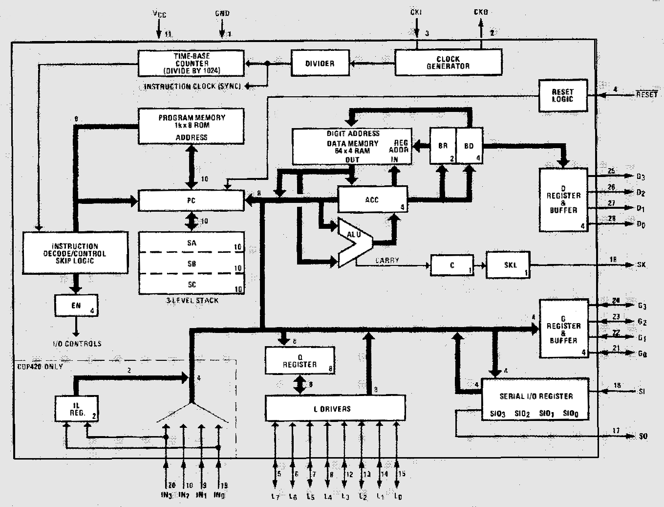
Test mode is entered by pulling the SO pin high with a 100 Ω resistor. During normal operation, SO is the output of the Serial I/O shift register, and it is low after Reset. This separates the Instruction Decode block from the ROM Program Memory (see block diagram above) and connects one of these to the Port L Drivers. Now we have two options: either we can insert instructions into Port L, which will be executed as if they would come from ROM (including incrementing the PC), or we could monitor the ROM contents without executing anything. The level at the SI pin decides what to do. High means instruction mode, low means ROM dump mode. The whole procedure is described in Application Note AB-4. Sounds easy, isn't it?
 |
 |
No, it isn't. There are two issues that render this task more difficult than expected. At first, timing. All input level changes have to be related to the SK pin, which provides an Instruction Clock signal. This pin is an output with a very bad slew rate. When inserting instructions, the L lines have to change 0..200 ns after the falling edge of SK. Second, which is not so clear in the beginning, there are a couple of errors in the timing diagram given in AB-4 FIGURE 3. And finally, there is a minimum clock rate of fCKI = 1.6 MHz required in the datasheet. Like most NMOS devices, the COP400 seems to use dynamic memory for its internal registers.
 Can we implement this in software on a microcontroller? There are two big issues: the latency from detecting the falling edge of SK to setting Port L would be much bigger than 200 ns, and the maximum clock frequency that could be achieved by toggling a pin would be around 500 kHz. This is 1/3 of the minimum required according to the datasheet.
Despite of the timing diagram given in the COP421 datasheet (see above), the block schematic indicates a fixed divider between CKI and SK. Therefore a preliminary test has been done: a 1 MHz signal has been applied to the CKI pin, the controller was set into test mode, and SK was observed with an oscilloscope. And there was a rectangular waveform with very bad risetime, acceptable fall time and exactly 1/16th of the clock frequency! An 1 kΩ pullup resistor at SK fixed the risetime, and now it was clear that all timing could be synchronized to CKI instead of SK. And we generate CKI ourself whereas we can only monitor SK. Now 500 kHz is still too slow compared to the 1.6 MHz reqired in the datasheet, but this is worth a try. Usually there is plenty of margin at room temperature -- a R6502 which is rated at 100 kHz to 1 MHz works fine at a couple of kilohertz.
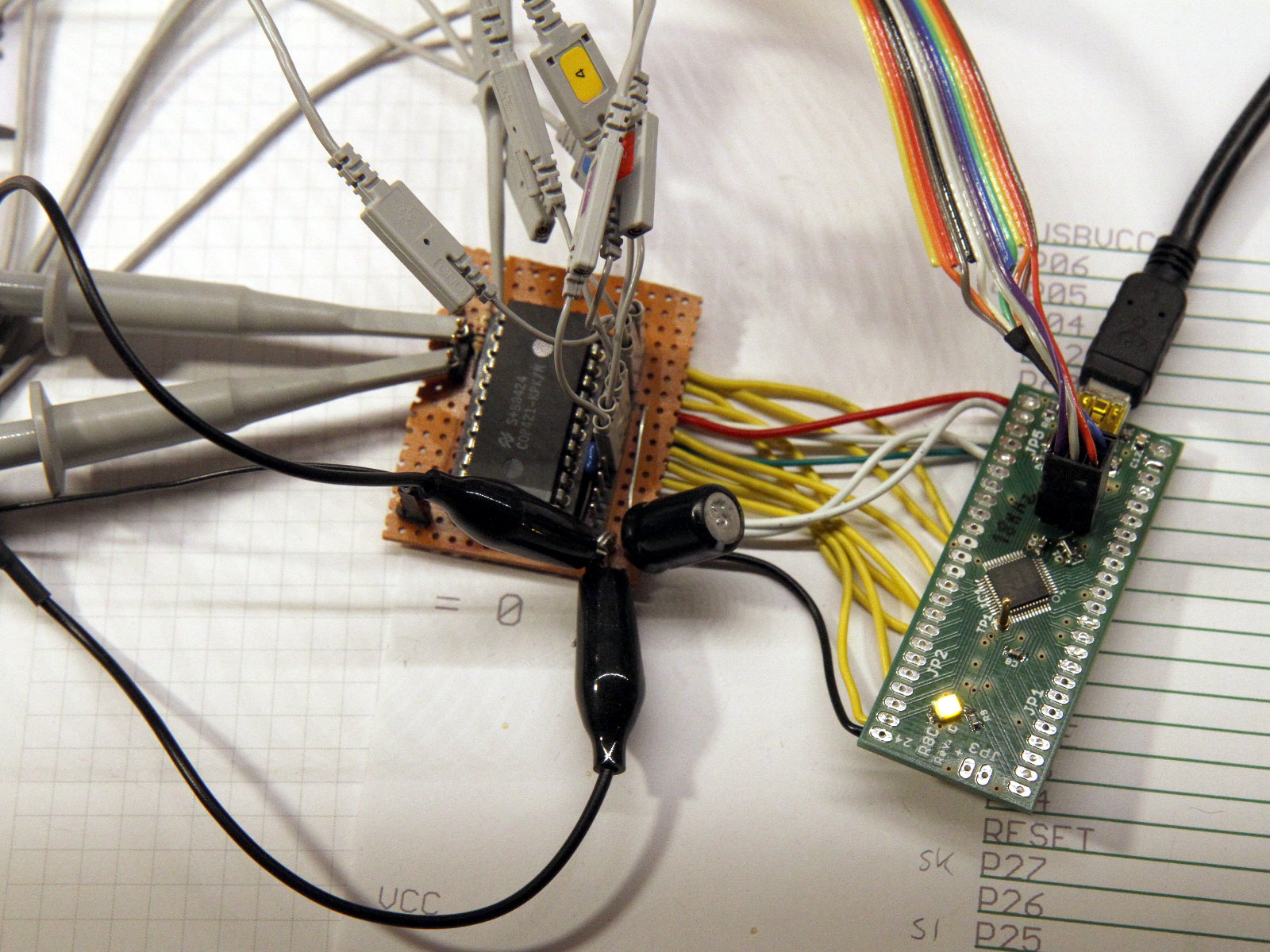
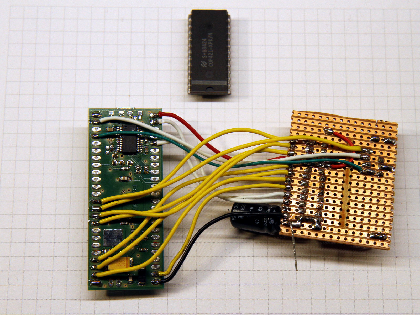
The COP400 ROM dumper consists of a Renesas R8C microcontroller that connects directly to the COPS Under Test ("CUT"). A generic module has been used which contains a R8C/348G controller, a FTDI FT232R serial-to-USB bridge, optional voltage regulator and support components. The CUT is placed onto a piece of prototype board and wired to the R8C according to the following table:
| signal | COP421 pin | R8C module pin | R8C pin |
|---|---|---|---|
| VDD | 9 | JP1.1, JP2.1 100 nF + 47 µF to Gnd |
- |
| Gnd | 1 | JP1.24, JP2.24 | - |
| CKI | 3 | JP2.5 | P2.1 |
| /RESET | 4 | JP2.2 | P2.4 |
| SK | 16 | JP1.21 1 kΩ to VDD |
P2.7 |
| SO | 15 | 100 Ω to VDD | - |
| SI | 14 | JP1.23 | P2.5 |
| L0 | 13 | JP1.12 | P0.0 |
| L1 | 12 | JP1.11 | P0.1 |
| L2 | 11 | JP1.10 | P0.2 |
| L3 | 10 | JP1.9 | P0.3 |
| L4 | 8 | JP1.4 | P0.4 |
| L5 | 7 | JP1.3 | P0.5 |
| L6 | 6 | JP1.2 | P0.6 |
| L7 | 5 | JP2.23 | P0.7 |
This is more or less a disposeable setup. After both COP421 masks have been recovered, I don't think I will ever need it again. Therefore it is only a quick & dirty mockup.
 |
 |
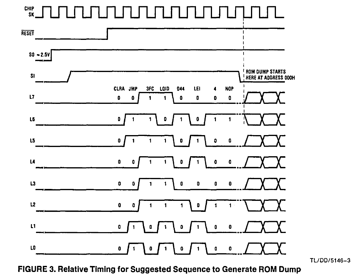
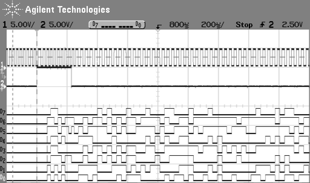
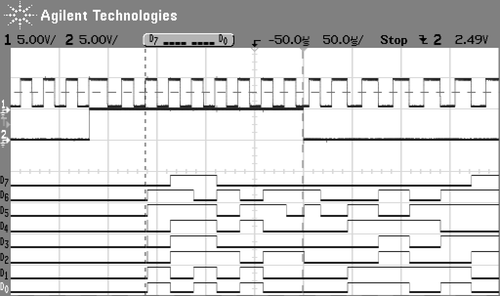
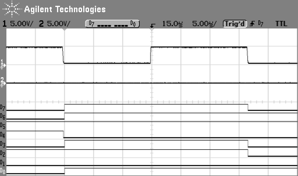
The whole test sequence has been implemented in software. At first, /Reset and SI are set low and clock cycles are generated for approximately 130 ms. This allows the controller to stabilize. SO is held high by the 100 Ω resistor. Then SI is set high to switch into instruction insertion mode. Again clock pulses are generated while monitoring SK, until the second rising edge is detected. Now the software is in sync with the rising edge of SK -- this is where the instruction byte should be applied to Port L. /Reset is deasserted and after 16 clock cycles (one SK period) the first instruction is applied. Again, 16 clock cycles, and the next instruction. This goes on until the whole test program has been transferred. The last command is a NOP (0x44), and in the middle of the low phase of its SK cycle (i.e. after 11 clocks) SI is set low to enter ROM dump mode. The following program code has been used:
 xxx:  00     CLRA           ; clear A. Every COP400 program has to start with this instruction.
 xxx:  63FC   JMP 0x3FC      ; set PC to 0x3FC
 3FC:  BF     LQID           ; transfer a ROM constant into Q. Usually this is indirectly addressed, but
 3FD:  44     db 0x44        ;   as ROM is disconnected, we have to provide the value here.
 3FE:  3364   LEI 0x4        ; set EN2 bit, which configures Port L as output with the value given in Q
 000:  44     NOP            ; we apply the same value from the other side...
        ... and set SI low to enter ROM dump mode at PC = 0x000.
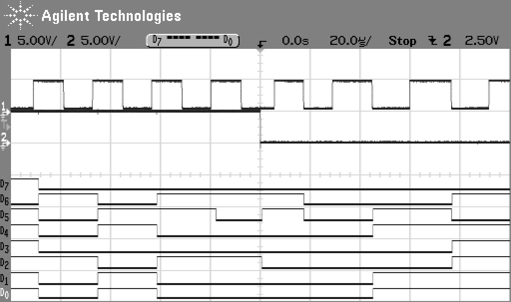
Note thet the opcode for LEI 0x4 is 3364, not 3344 as stated in the application note. Besides that, SI must be switched low during the SK low phase of the NOP instruction itself, not in the next cycle. With the timing given in FIGURE 3 of AB-4, the ROM dump would start at address 0x001, i.e. the first byte is missing. Even with unknown ROM code, it is possible to recognize this condition because every COP400 program has to start with a CLRA (0x00) instruction. The correct timing is shown in the oscilloscope screenshots below:
 |
 |
 |
 |
The ROM dumper program reads 2048 bytes which is the maximum size for the COP400 architecture. This means for a COP421 the ROM code will appear twice, but in case a 2 kB COP444 needs to be dumped this will also be possible. The microcontroller is operated at an average clock of 500 kHz, which is outside its specification. However, as expected before there is a lot of margin. During my experiments the clock could be stopped for nearly one second before the controller died and required a /Reset to come back.
Both Lisa COP421 controllers have been dumped, I have send the image files and disassemblies to bitsavers.org. Therefore I don't expect anyone to feel the necessity to recreate my setup. I will keep it for some time (until I need the parts ;-), so just contact me if you have a controller to be read. Anyway, here are the project files:
a) Renesas R8C module. This is the same board as used for UsbWidEx.
b) Object code.
The smallest R8C/34 with 32 kB can be used here, the program is very short. Besides UART0, no special periphery is used. Therefore the code should run on other R8C types, too. Refer to my UsbWidEx article for a description of the flash procedure.
Here is the recording of a sample session, just to give an impression of the user interface. The R8C board is connected to an USB port and a terminal window has been opened for the virtual COM port. With Windows 7 / 64 bit I use TeraTerm. The RS-232 settings are 57600-8-1, no handshake. After the first keypress, the welcome message appears:
COPSreader V0.99
 (c) Patrick Schaefer, 2016

  1 - read COP400 ROM
  2 - print hex dump
  3 - print Intel Hex file
Select function:
Pressing "1" starts the ROM read sequence.
reading COP421 ...done.
Now the ROM mask has been transferred into a buffer. It can be printed either as a hex dump
COPSreader V0.99
(c) Patrick Schaefer, 2016
1 - read COP400 ROM
2 - print hex dump
3 - print Intel Hex file
Select function: 2
Data Buffer:
0000: 00335F326BEC20CC 324F22CD4F2162F8 .3_2kì Ì2O"ÍO!bø
0010: 6A5620D98C2D7F7E 8F684069FA687768 jV Ù-~.h@iúhwh
0020: 406924684041EB6A 7B69BE68FFD96019 @i$h@Aëj{i¾hÿÙ`.
0030: 7361697369737361 6173736973696173 saisissaassisias
(...)
07E0: AA33616329336DAA 336563290F005F06 ª3ac)3mª3ec).._.
07F0: 153600160034ED61 E52300063FAB3360 .6...4íaå#..?«3`
or in Intel Hex format for further processing
COPSreader V0.99
 (c) Patrick Schaefer, 2016

  1 - read COP400 ROM
  2 - print hex dump
  3 - print Intel Hex file
Select function: 3


:1000000000335F326BEC20CC324F22CD4F2162F8AF
:100010006A5620D98C2D7F7E8F684069FA68776890
:10002000406924684041EB6A7B69BE68FFD960196A
  (...)
:1007F000153600160034ED61E52300063FAB33608B
:00000001FF
That's all. Note that always 2048 bytes are read. Therefore the ROM contents of a COP410/411 will repeat four times, a COP420/421 two times and only a COP444 will fill the whole buffer area.
I did not find a freeware disassembler for COP400 microcontrollers. In fact, I did not find any at all. There seems to be some kind of COP400 emulator inside the MAME arcade machine emulator code. So if anyone wants to write one, this may be a starting point. The two Apple masks have been disassembled manually. This is more or less a find & replace job. Every hex number represents an instruction, except for 0x60..0x6F and 0x33 -- these are two byte instructions. Each COP400 program has to start with 0x00, empty space is 0x00, and NOP is 0x44. Alfred's as assembler can be used to convert the disassembly back into COPS code. For a plausibility check, or if someone wants to design a new ROM mask. Have fun!
An Update: In January 2016 there was no COPS400 disassembler -- well there is one now :-). Analyzing some HP-IL peripherals (which also use National microcontrollers), Dr. Vassilis Prevelakis wrote cop4disass, a disassembler for the COP402. The source is on github: https://github.com/vp080808/COP4-Disassembler. cop4disass produces output compatible with the as macro assembler.
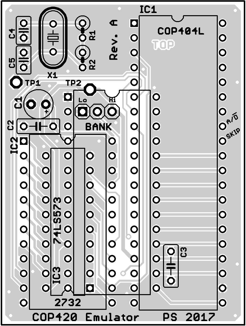
To allow software development and testing, National offered thee ROMless COP4 devices: COP402, COP402M and COP404L. These have a DIP-40 package. 28 of the 40 pins provide the same function as for a COP420, the other twelve connect to an external 2kB 2716-type EPROM. Address and data lines are multiplexed, therefore a 74LS573 is needed to latch the lower address byte. All three ROMless devices are similar, but there are small differences that could have an impact on their ability to replace a given mask ROM controller:
| Type | internal RAM |
external ROM |
Vcc range | max. clock frequency cycle time |
Compatibility |
|---|---|---|---|---|---|
| COP402, KR1820VE1A | 64 x4 bit | up to 1 kByte | 4.5 to 6.3 V | 4 MHz, Crystal /16 (> 4 µs) |
COP420, COP421, COP422 |
| COP402M | 64 x4 bit | up to 1 kByte | 4.5 to 6.3 V | 4 MHz, Crystal /16 (> 4 µs) |
COP420, COP421, COP422 with Microbus option |
| COP404LSN-5 | 128 x4 bit | up to 2 kByte | 4.5 to 5.5 V | 2 MHz, Crystal /32 (> 16 µs) |
COP444L, COP420L, COP421L low power devices |
The Russian KR1820VE1A (in cyrillic letters "KP1820BE1A") is a second-source for the COP402. It is sold quite often on ebay, so it might be easier to get. However, this part has a metric 2.50 mm pitch instead of the common 2.54 mm (0.1"). Therefore it does not fit into "precision" sockets with turned contacts. "Cheap" sockets with straight spring contacts forgive the missing 0.76 mm, and direct soldering into the PCB will also work.
Here are two emulator boards that allow substitution of 28 pin resp. 24 pin mask ROM devices with a 40 pin ROMless device plus EPROM. They can be used to test software modifications, trace program flow by monitoring the ROM address lines, or just to replace broken COP4 mask ROM chips. Use a COP402 to substitute 4 MHz COP420/421/422 and a COP404LSN-5 as a replacement for 2 MHz low-power devices.
 |
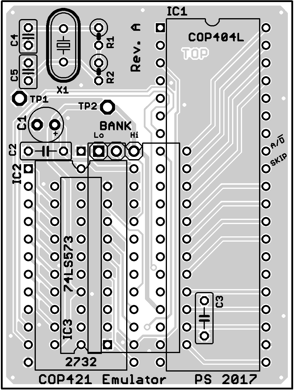 |
There is no schematic diagram, the wiring is exactly as recommended in the COP404L datasheet. I have used a 74LS (or 'HCT) 573 instead of the 74LS373 because its pin order made routing easier. For the EPROM, either a 2716 or 2732 with access time below 1000 ns (yes, one microsecond!) can be used. With a 2716, set the BANK jumper to the Hi position (connecting /PGM to VDD). For a 2732, use it to select the upper or lower 2k bank (A11 high or low). Testpoint TP1 is Gnd, TP2 is VDD. Fit 10 .. 47 µF / 16 V for C1 and 100 nF for C2 and C3.
Note that the 74LS573 is upside down and needs to be fitted below the EPROM, which of course has to be put into a socket. If you use a COP402 controller, duplicate the ROM image to fill the whole 2 kB area of the EPROM. This is because A10 is driven from pin 32 of the controller socket. For a COP404L this is A10, but the COP402 uses this pin to provide a SKIP signal that indicates a contitional branch (SKIP instruction) has been taken. Therefore this pin can be high or low depending on the program flow. Duplicating the 1k ROM image makes A10 don't care, i.e. the controller will address the same memory location for both states.
Standard COP4 controllers have a minimum instruction cycle time of 4 µs, i.e. a maximum clock frequency of 250 kHz. CPU clock is generated by dividing the external clock source (crystal, RC, TTL signal) by 16, by 8 or by 4. This ratio is set by ROM Option 3. The ROMless devices have a fixed ratio of 16 (COP402) or 32 (COP404L), therefore your emulator might need a different clock source than your target. For that case, a Pierce tank circuit is provided on the board. Chose the components according to the required frequency.
| X1 / MHz | R1 / kOhm | R2 / MOhm | C4 / pF | C5 / pF | from datasheet |
|---|---|---|---|---|---|
| 4 | 4.7 | 1 | 22 | 22 | COP420 |
| 3.58 | 3.3 | 1 | 22 | 27 | COP420 |
| 2.097 | 8.2 | 1 | 47 | 33 | COP420 |
| 2.097 | 1 | 1 | 56 | 6..36 | COP404L |
In case you prefer the Colpitts circuit shown in earlier revisions of the datasheets, cut the traces between C5, X1 and R2 and re-wire them accordingly. On the bottom of the PCB are two solder bridges that connect CKO and CKI either to the tank circuit or to pin 2 and 3 of the target connector. The pictures below show an assembled COP421 emulator board used to replace the COP421-HZT/N on the I/O board of a Lisa 2/5.
 |
 |
As usual: I will give absolutely no guarantee that the software or circuit will work as described, that it will not destroy your computer, the circuit itself, or any peripherials connected to it. I also refuse any responsibilty for data losses resulting from the use of this software and circuit design. It's freeware. If you want some guarantee, buy a commerial product. It is explicitly prohibited to use the software and circuit described here in places where failure or malfunction may be dangerous to the health or result in monetary losses.
COPSreader and the COP4 emulator layouts are copyright (c) by Dr. Patrick Schäfer, 2016 - 2017
Apple, Lisa and the COP421-KPK and -HZT masks are (c) by Apple Computer Inc.
----> Back to my home page