ProFile, Widget and Nisha are controlled by one or more Zilog Z8 microcontrollers with fixed mask ROM. Mask ROM is a cheap and reliable solution for series production, but as its contents cannot be changed anymore it is not suitable for software development. And sometimes it is necessary to modify or replace the drive firmware, e.g. for low-level formatting or troubleshooting! Therefore some kind of emulator device is needed.
When the Z8 microcontroller family was introduced in 1979, Flash memory was not invented yet. Internal memory was mask ROM, and for software development either external EPROM memory or an in-circuit emulator system was used. Zilog offered two different mask ROM controllers, the Z8601 with 2kB and the Z8611 with 4kB ROM. For software development, two special prototyping devices were available, which had an external EPROM sitting on the back of the chip. These "Piggyback" devices were the Z8603 (with 2kB 2716) and Z8613 (with 4kB 2732). Both are very difficult to obtain today. Later, on-chip mask ROM was complemented by EPROM technology. The Z86E21 is pin compatible to the old Z801 and Z8611 mask ROM devices. It has 8kB EPROM memory and is available in OTP plastic and UV-eraseable cerdip packages. However, it needs a special programmer (like my old Data I/O Sprint Expert) and it can only be used in applications where external memory does not start below $2000. Widget has 4kB of external memory located at $1000 which would be overlapped by the internal ROM.
Today's Z8encore devices use flash memory, but they are based on the faster eZ8 core. Therefore their runtime behaviour is different from the original series and they cannot be used as a replacement.
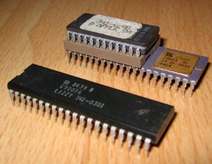
So it seems to be difficult. But fortunately there is another option: Official sources for the Z8 devices were Zilog themselves, Synertek, and SGS (now STMicroelectronics). However, there was another company that made functionally compatible devices: the East German VEB Kombinat Mikroelektronik "Karl Marx" (MME) located in Erfurt, GDR. During Cold War times they did not get a regular second source licence, therefore some creative reverse engineering was necessary. The result was the U881 (order code UB8810D) which is similar to the Z8601. U882 (2kB, order code UB8820M) and U884 (4kB, order code UB8840M) were the ROMless variants. These were housed in a strange-looking 64 pin quad in line (QIL) package.
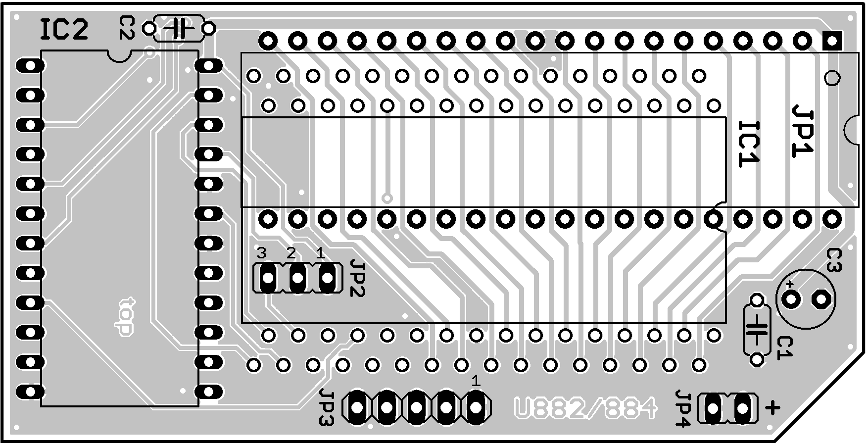
From functional point of view, MME's ROMless single-chip microcontrollers U882 and U884 are identical to Zilog/SGS's piggyback devices Z8603 and Z8613. However, they have a flat 64 pin package, therefore a PCB is required to connect the EPROM and to provide an interface into the 40 pin Z8 socket. There is no schematic diagram because the circuit is straight-forward.
IC1 is the U882 or U884 device. Which one you need depends on your application. The U884 has 4kB internal memory, which sounds better at first. However, having this memory internally blocks any external memory or I/O in this area. So it cannot be used in applications where anything external starts below $1000. IC2 is the EPROM device. Depending on IC1, a 2716 (2kB) or 2732 (4kB) has to be used here. JP1 connects into the Z8 socket, therefore it has to be mounted on the bottom side of the board. JP2 defines the connection of IC2's A11 line:
| IC1 type | EPROM type | JP2 setting |
| UB8820 (2kB) | 2716 | 1-2 |
| UB8820 (2kB) | 2732 (lower 2kB) | 2-3 |
| UB8820 (2kB) | 2732 (upper 2kB) | 1-2 |
| UB8840 (4kB) | 2732 (4kB) | 2-3 |
In a fixed configuration, JP2 can be substituted by a wire. Otherwise mount it on the bottom side and use a very flat jumper type. For those of you, who want to etch their own board, here are the necessary files available for download:
JP3 and JP4 are not needed during regular operation. Thanks to its 64 pin package the U882 provides some additional signals which are not available with the Z8603. These signals may be used together with a logic analyzer to get a deeper insight into the Z8's internal operation.
| Pin | Signal | Function |
| JP3.1 | Gnd | Ground |
| JP3.2 | IACK | Interrupt Acknowledge. High during all machine cycles of an interrupt acknowledge. |
| JP3.3 | /SYNC | Instruction Synchronisation. Low before the first byte of a machine instruction is fetched. |
| JP3.4 | SCLK | System Clock. This is the XTAL frequency divided by 2. |
| JP3.5 | /MDS | Program Memory Data Strobe. Low whenever an instruction is fetched from internal memory. Not active during constant fetch or interrupt acknowledge. |
| JP4.1 | VCC | +5 Volt supply voltage |
| JP4.2 | Gnd | Ground |
To keep the module compact, several components had to be placed on the bottom side of the PCB. This results in a certain order in which the components have to be assembled. Start with the first half of JP1. Insert the pin header into the board, solder it, and cut the protruding ends on the top to get a flat surface for the U882. Next, insert JP2 from the bottom and solder it. JP2 needs to be low profile to avoid collisions with the parts on your application board. With an U884 JP2 can be substituted by a wire (there is only one valid position). With an U882 it depends on whether you want to be able to use a 2732 or not.
 |
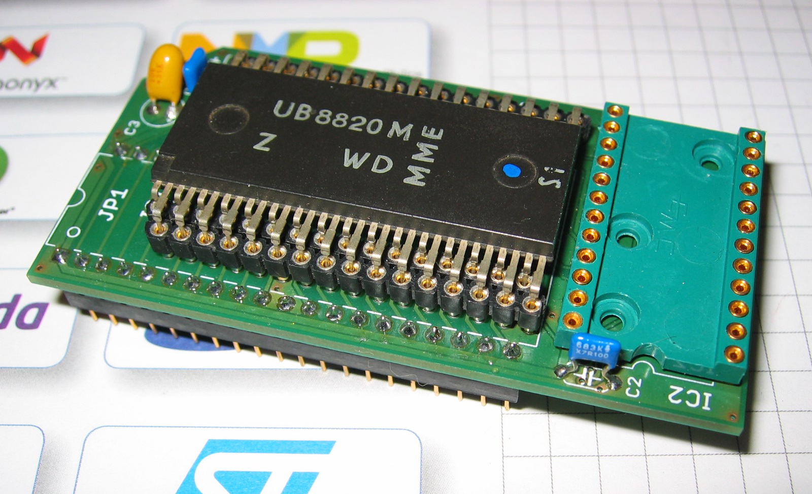 |
Now insert the U882 himself and solder it to the board. Make sure to get the correct orientation! It is possible to build a socket for IC1 (as I did on the picture above), but be warned: it is very diffiult to insert the chip into the socket without bending its pins, and it is even more difficult to remove it from there without severely bending or breaking them! As long as you do not plan to change the chip regularly, solder it directly to the board.
After that, the rest of the components can be fitted.
To use the U882 board in your application, put an EPROM with the contents of the target Z8's internal memory into IC2 or connect the IC2 socket to your EPROM emulator and load the target file. Make sure that JP2 is set correctly, then put the board into the application Z8 socket. Re-check its orientation twice, then apply power. Now your application should start up as usual.
In case it does not, check if half of the Xtal frequency can be measured at the SCLK pad (JP3.4). If the crystal oscillator in your application circuit is not able to drive the board, use a different clock source which provides a buffered signal.
The photos below show the U882 board fitted inside a ProFile drive. It is small enough to allow the top cover to be mounted, so it can be used as a permanent replacement for a broken 341-0080-B Z8 chip.
 |
 |
According to Zilog's 1985 data book, the EPROM for an 8 MHz Z8 should have an access time TdA(DI) of 460ns or faster. With 5 MHz, up to 830ns are allowed.
As usual: I will give absolutely no guarantee that the software or circuit will work as described, that it will not destroy your computer, the circuit itself, or any peripherials connected to it. I also refuse any responsibilty for data losses resulting from the use of this software and circuit design. It's freeware. If you want some guarantee, buy a commerial product. It is explicitly prohibited to use the software and circuit described here in places where failure or malfunction may be dangerous to the health or result in monetary losses.
Z8 Piggyback Replacement is copyright (c) by Dr. Patrick Schäfer, 2012
----> Back to my home page